


-
- Elektronik (Wafer, Halbleiter, Mikrochips,...)
New partnership enables an innovative network together with academia and industry partners to strengthen digital sovereignty in Europe
Baden-Württemberg attracts imec to lead development of chiplet-based technology for automotive applications
Imec, a world-leading research and innovation hub in nanoelectronics and digital technologies, and the State Government of Baden-Württemberg, Germany, today announced, at the Hannover Trade Fair, the launch of the Advanced Chip Design Accelerator (ACDA). The new imec competence center in Baden-Wür…


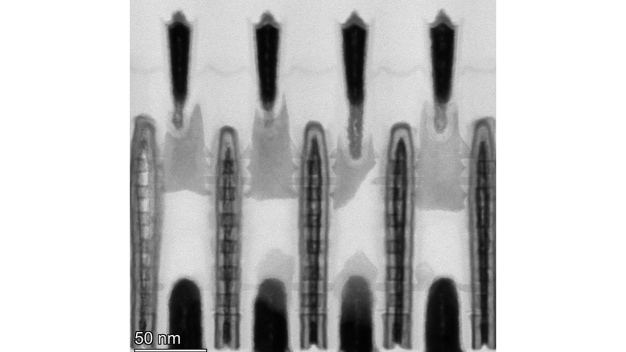
 und Gabeln (rechts) mit 20 nm Abstand nach der Musterübertragung in eine TiN-Hartmaske. / Figure 1 - Top-down SEM pictures of 20nm pitch meanders (left) and forks (right) after pattern transfer into TiN hard mask.")
. / Figure 2 - TEM picture of metallized 20nm pitch wires after a chemical mechanical polishing (CMP) step.")


 eines einreihigen CFET und (b) eines zweireihigen CFET. Das Layout eines Flipflops (D-Flipflop oder DFF) zeigt eine Verringerung der Zellenhöhe und -fläche um 24 nm (oder 12,5 %) beim Übergang von einem einreihigen zu einem zweireihigen CFET (H. Kuekner et al., IEDM 2024). / Figure 1 – Conceptual representation of (a) a single-row CFET and (b) a double-row CFET. The layout of a flip-flop (D-type flip-flop or DFF) shows a reduction of the cell height & area with 24nm (or 12.5%) when transitioning from a single-row to a double-row CFET (H. Kuekner et al., IEDM 2024).")
. Die Detailansicht zeigt ein TEM eines monolithischen CFET-Technologie-Demonstrators, der in der 300-mm-Reinraum-F&E-Einrichtung von imec hergestellt wurde (A. Vandooren et al., IEDM 2024). / Figure 2 – Virtual process flow for building a double-row CFET architecture. The process flow, simulated with 3D Coventor, started from the specifications of a ‘virtual’ CFET fab, projecting future processing capabilities and design margins (H. Kuekner et al., IEDM 2024). The zoom-in represents a TEM of a monolithic CFET technology demonstrator fabricated within imec’s 300mm R&D cleanroom facility (A. Vandooren et al., IEDM 2024).")

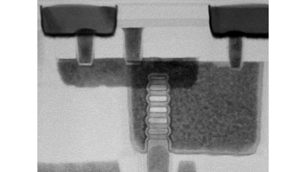
. Gezeigt werden REM-Querschnitte längs (links) und quer (rechts) zum BC/TC. / Figure 1 – CMOS CFET devices with MDI and stacked frontside patterned contacts (TC = top contact; TJ = top junction; BC = bottom contact; BJ = bottom junction). SEM cross sections are shown along (left) and across (right) the BC/TC.")

. / Figure 3 – SEM picture showing bottom contacts formed on the wafer backside and positioned accurately over the bottom junction formed on the frontside (BDI = bottom dielectric isolation).")


 Vision für ein optisch verbundenes Multi-XPU-Rechnersystem auf Waferebene; und B) demonstriertes Testsystem, das aus PIC-Dies mit eingebetteten SiN-Wellenleitern (WG) und evaneszenten Kopplern besteht, die mit einem unteren PIC-Wafer mit komplementären SiN-evaneszenten Kopplern verbunden sind. / Figure 2 – A) Vision for a wafer-level, optically interconnected multi-XPU compute system; and B) demonstrated test system comprising of PIC dies with embedded SiN waveguides (WG) and evanescent couplers bonded to a bottom PIC wafer with complementary SiN evanescent couplers.")

 Schematischer Querschnitt des Chip-Schichtstapels, der die Lichteinkopplung in den Chip, die Beleuchtung der Zellen sowie die Erfassung und Detektion der Zellstreusignale zeigt. (rechts) Experimentelles Streudiagramm einer vollständigen mononukleären Probe aus peripherem Blut, gemessen mit dem On-Chip-Durchflusszytometer. / Figure 2: (Left) Schematic cross-section of the chip layer stack, indicating light coupling into the chip, cell illumination, and collection and detection of cell scattering signals. (Right) Experimental scatter plot of a full peripheral blood mononuclear sample measured with the on-chip flow cytometer.")


