


-
- Electronics (wafers, semiconductors, microchips,...)
Milestone in semiconductor development
New semiconductor material: AlYN promises more energy-efficient and powerful electronics
Researchers at Fraunhofer IAF have made a breakthrough in the field of semiconductor materials: With aluminum yttrium nitride (AlYN), they have succeeded in fabricating and characterizing a new and promising semiconductor material using the MOCVD process. Due to its excellent material properties and…


")

")


")
")
")
")
")


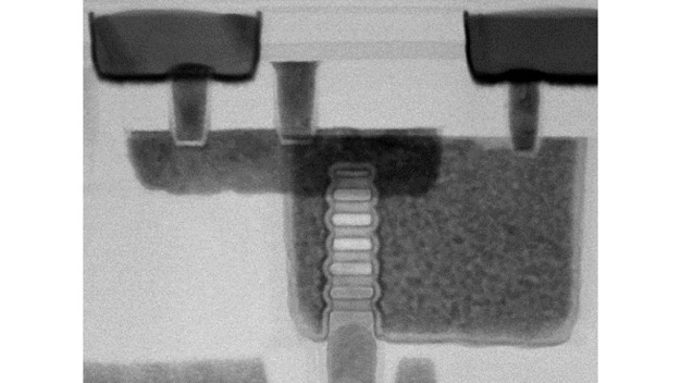
. Gezeigt werden REM-Querschnitte längs (links) und quer (rechts) zum BC/TC. / Figure 1 – CMOS CFET devices with MDI and stacked frontside patterned contacts (TC = top contact; TJ = top junction; BC = bottom contact; BJ = bottom junction). SEM cross sections are shown along (left) and across (right) the BC/TC.")

. / Figure 3 – SEM picture showing bottom contacts formed on the wafer backside and positioned accurately over the bottom junction formed on the frontside (BDI = bottom dielectric isolation).")
![Mitarbeitende von EV Group und des Fraunhofer IZM-ASSID neben einem vollautomatischen EVG®850 DB UV-Laser-Debonding- und Reinigungssystem, installiert im neu eröffneten Center for Advanced CMOS and Heterointegration Saxony (CEASAX) von Fraunhofer in Dresden, Deutschland. [Vin links nach recths: Gerald Silberer, Regional Sales Director Europe (EV Group), Dr. Andreas Gang, Group Leader Pre-Assembly / Wafer Bonding (Fraunhofer IZM-ASSID), Dr. Manuela Junghähnel, Site Manager (Fraunhofer IZM-ASSID), Markus Wimplinger, Corporate Technology Development & IP Director (EV Group), Andreas Pichler, Regional Sales Manager Europe (EV Group), Robert Wendling, Technical Assistant Wafer Bonding (Fraunhofer IZM-ASSID), Dr. Frank Windrich, Deputy Site Manager (Fraunhofer IZM-ASSID)]. © Fraunhofer IZM | Silvia Wolf / EV Group and Fraunhofer IZM-ASSID personnel next to an EVG®850 DB fully automated UV laser debonding and cleaning system installed in Fraunhofer’s newly established Center for Advanced CMOS and Heterointegration Saxony (CEASAX) in Dresden, Germany. [From left to right: Gerald Silberer, Regional Sales Director Europe (EV Group), Dr. Andreas Gang, Group Leader Pre-Assembly / Wafer Bonding (Fraunhofer IZM-ASSID), Dr. Manuela Junghähnel, Site Manager (Fraunhofer IZM-ASSID), Markus Wimplinger, Corporate Technology Development & IP Director (EV Group), Andreas Pichler, Regional Sales Manager Europe (EV Group), Robert Wendling, Technical Assistant Wafer Bonding (Fraunhofer IZM-ASSID), Dr. Frank Windrich, Deputy Site Manager (Fraunhofer IZM-ASSID)]. © Fraunhofer IZM | Silvia Wolf](/uploads/images/_scale/dsc4037klein_169_626x352.jpg "Mitarbeitende von EV Group und des Fraunhofer IZM-ASSID neben einem vollautomatischen EVG®850 DB UV-Laser-Debonding- und Reinigungssystem, installiert im neu eröffneten Center for Advanced CMOS and Heterointegration Saxony (CEASAX) von Fraunhofer in Dresden, Deutschland. [Vin links nach recths: Gerald Silberer, Regional Sales Director Europe (EV Group), Dr. Andreas Gang, Group Leader Pre-Assembly / Wafer Bonding (Fraunhofer IZM-ASSID), Dr. Manuela Junghähnel, Site Manager (Fraunhofer IZM-ASSID), Markus Wimplinger, Corporate Technology Development & IP Director (EV Group), Andreas Pichler, Regional Sales Manager Europe (EV Group), Robert Wendling, Technical Assistant Wafer Bonding (Fraunhofer IZM-ASSID), Dr. Frank Windrich, Deputy Site Manager (Fraunhofer IZM-ASSID)]. © Fraunhofer IZM | Silvia Wolf / EV Group and Fraunhofer IZM-ASSID personnel next to an EVG®850 DB fully automated UV laser debonding and cleaning system installed in Fraunhofer’s newly established Center for Advanced CMOS and Heterointegration Saxony (CEASAX) in Dresden, Germany. [From left to right: Gerald Silberer, Regional Sales Director Europe (EV Group), Dr. Andreas Gang, Group Leader Pre-Assembly / Wafer Bonding (Fraunhofer IZM-ASSID), Dr. Manuela Junghähnel, Site Manager (Fraunhofer IZM-ASSID), Markus Wimplinger, Corporate Technology Development & IP Director (EV Group), Andreas Pichler, Regional Sales Manager Europe (EV Group), Robert Wendling, Technical Assistant Wafer Bonding (Fraunhofer IZM-ASSID), Dr. Frank Windrich, Deputy Site Manager (Fraunhofer IZM-ASSID)]. © Fraunhofer IZM | Silvia Wolf")


