Here you can find the NEWSLETTER archive More ...
Vaisala Buchta HJM C-Tec

cleanroom online
Deutsch   English


All publications for the rubric Electronics (wafers, semiconductors, microchips,...)

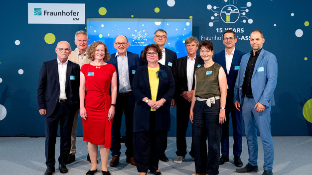
Mitarbeitende von EV Group und des Fraunhofer IZM-ASSID neben einem vollautomatischen EVG®850 DB UV-Laser-Debonding- und Reinigungssystem, installiert im neu eröffneten Center for Advanced CMOS and Heterointegration Saxony (CEASAX) von Fraunhofer in Dresden, Deutschland. [Vin links nach recths: Gerald Silberer, Regional Sales Director Europe (EV Group), Dr. Andreas Gang, Group Leader Pre-Assembly / Wafer Bonding (Fraunhofer IZM-ASSID), Dr. Manuela Junghähnel, Site Manager (Fraunhofer IZM-ASSID), Markus Wimplinger, Corporate Technology Development & IP Director (EV Group), Andreas Pichler, Regional Sales Manager Europe (EV Group), Robert Wendling, Technical Assistant Wafer Bonding (Fraunhofer IZM-ASSID), Dr. Frank Windrich, Deputy Site Manager (Fraunhofer IZM-ASSID)]. © Fraunhofer IZM | Silvia Wolf / EV Group and Fraunhofer IZM-ASSID personnel next to an EVG®850 DB fully automated UV laser debonding and cleaning system installed in Fraunhofer’s newly established Center for Advanced CMOS and Heterointegration Saxony (CEASAX) in Dresden, Germany. [From left to right: Gerald Silberer, Regional Sales Director Europe (EV Group), Dr. Andreas Gang, Group Leader Pre-Assembly / Wafer Bonding (Fraunhofer IZM-ASSID), Dr. Manuela Junghähnel, Site Manager (Fraunhofer IZM-ASSID), Markus Wimplinger, Corporate Technology Development & IP Director (EV Group), Andreas Pichler, Regional Sales Manager Europe (EV Group), Robert Wendling, Technical Assistant Wafer Bonding (Fraunhofer IZM-ASSID), Dr. Frank Windrich, Deputy Site Manager (Fraunhofer IZM-ASSID)]. © Fraunhofer IZM | Silvia Wolf
  • Electronics (wafers, semiconductors, microchips,...)

ST. FLORIAN, Austria and MORITZBURG, Germany Strategic partnership kicks off with installation of EVG850 automated laser debonding system at the newly launched Center for Advanced CMOS and Heterointegration Saxony (CEASAX)

EV Group and Fraunhofer IZM-ASSID expand partnership in Wafer Bonding for Quantum Computing applications

EV Group (EVG), a leading supplier of wafer bonding and lithography equipment for the MEMS, nanotechnology and semiconductor markets, and Fraunhofer IZM-ASSID (All Silicon System Integration Dresden), a division of Fraunhofer IZM that provides world-leading applied research in semiconductor 3D wafer…

The TWINSCAN EXE:5000 High NA EUV scanner in the High NA Lab demonstrating the first-ever 10 nm dense lines obtained in a single exposure.
  • Electronics (wafers, semiconductors, microchips,...)

Opening of the joint ASML-imec High NA EUV Lithography Lab marks a milestone in preparing High NA EUV lithography for accelerated adoption in mass manufacturing

ASML and imec open joint High NA EUV Lithography Lab offering an early development platform to the leading-edge semiconductor ecosystem

Imec, a world-leading research and innovation hub in nanoelectronics and digital technologies, and ASML Holding N.V. (ASML), a leading lithography supplier to the semiconductor industry, today announced the opening of the High NA EUV Lithography Lab in Veldhoven, the Netherlands, a lab jointly run b…

Abbildung 1 - SEM- Querschnittsaufnahme eines Die-to-Wafer hybrid gebondeten Versuchsträgers mit 2µm Bondpadabstand. / Figure 1 – Cross-section SEM image of a die-to-wafer hybrid bonded test vehicle with 2µm bond pad pitch. Abbildung 2 - A) Vision für ein optisch verbundenes Multi-XPU-Rechnersystem auf Waferebene; und B) demonstriertes Testsystem, das aus PIC-Dies mit eingebetteten SiN-Wellenleitern (WG) und evaneszenten Kopplern besteht, die mit einem unteren PIC-Wafer mit komplementären SiN-evaneszenten Kopplern verbunden sind. / Figure 2 – A) Vision for a wafer-level, optically interconnected multi-XPU compute system; and B) demonstrated test system comprising of PIC dies with embedded SiN waveguides (WG) and evanescent couplers bonded to a bottom PIC wafer with complementary SiN evanescent couplers.
  • Electronics (wafers, semiconductors, microchips,...)

Improved die-to-wafer assembly flow opens doors to logic/memory-on-logic stacking, and to optically interconnected systems-on-wafer

Imec demonstrates die-to-wafer hybrid bonding with a Cu interconnect pad pitch of 2µm

This week, at the 2024 IEEE Electronic Components and Technology Conference (ECTC), imec, a world-leading research and innovation hub in nanoelectronics and digital technologies, presents a Cu-to-Cu and SiCN-to-SiCN die-to-wafer bonding process resulting in a Cu bond pad pitch of only 2µm at <35…

300-mm-Reinraum des Fraunhofer IPMS.  © Fraunhofer IPMS / 300 mm cleanroom at the Fraunhofer IPMS. © Fraunhofer IPMS Luftbildaufnahme von Infineon Dresden. © Infineon Technologies AG / Aerial view of Infineon Dresden. © Infineon Technologies AG „Smart-Power-Technologien“ in Anwendungen für Endverbraucher. © Infineon Technologies AG /
  • Electronics (wafers, semiconductors, microchips,...)

Intelligent energy management for the future

Fraunhofer IPMS supports the 300 mm process development of smart power technologies for the semiconductor manufacturer Infineon at the Dresden site

In a joint development project spanning around one year, important progress was made in the production of “Smart power technologies”. Fraunhofer IPMS provided significant support to the semiconductor manufacturer Infineon by supplying selected process modules within the entire CMOS process value…

5DOF Miniatur-XYZ-Phi-Delta Positioniersystem für die aktive Ausrichtung und Montage von Optiken. (Copyright: Steinmeyer Mechatronik)
  • Electronics (wafers, semiconductors, microchips,...)

Hochpräzises Positioniersystem für die aktive Ausrichtung und Montage von Optiken

Innovativer 5-Achs-Aligner für die Halbleiterindustrie

Mit dem 5DOF Miniatur-XYZ-Phi-Delta Positioniersystem bietet Steinmeyer Mechatronik eine innovative Lösung für hochpräzise Ausrichtprozesse. Die Kombination aus Tripod und XY-Kreuztisch gewährleistet ein Höchstmaß an Präzision, Robustheit sowie Zuverlässigkeit und begeistert gleichzeitig mit…

Better informed: With YEARBOOK, NEWSLETTER, NEWSFLASH and EXPERT DIRECTORY

Stay up to date and subscribe to our monthly eMail-NEWSLETTER and our NEWSFLASH. Get additional information about what is happening in the world of cleanrooms with our printed YEARBOOK. And find out who the cleanroom EXPERTS are with our directory.

ASYS ClearClean MT-Messtechnik Hydroflex